Journal of The Electrochemical Society, 156 ͑12͒ G201-G205 ͑2009͒
G205
1
1
Defects in Silicon, W. M. Bullis and L. C. Kimerling, PV83-9, p. 629, The Elec-
trochemical Society Proceedings Series, Pennington, NJ ͑1983͒.
. J. Ryuta, E. Morita, T. Tanaka, and Y. Shimanuki, Jpn. J. Appl. Phys., Part 2, 29,
L1947 ͑1990͒.
. K. Yamabe and K. Taniguchi, IEEE Trans. Electron Devices, ED-32, 423 ͑1985͒;
K. Yamabe and K. Taniguchi, IEEE J. Solid-State Circuits, SC-20, 343 ͑1985͒.
. R. Hasunuma, J. Okamoto, N. Tokuda, and K. Yamabe, Jpn. J. Appl. Phys., Part 1,
rounding-off oxidation model at the Si trench corner, and this sup-
pression of the oxidation stress can expand the incubation region.
2
3
4
5
Conclusion
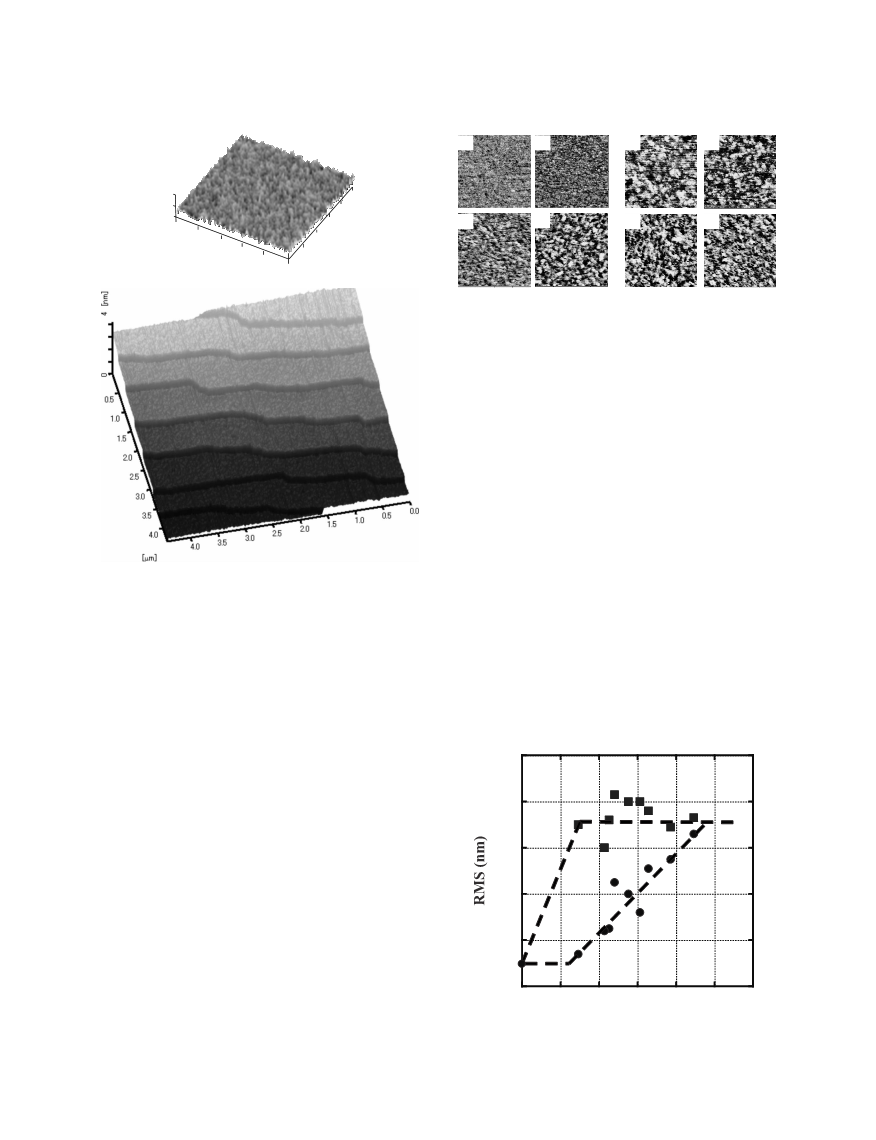
In summary, an atomically flat Si surface enabled us to investi-
gate the atomistic phenomena of thermal oxidation. As a result,
some of the following phenomena are clarified. The SiO surface
roughness gradually increases before saturation. In the initial rapid
oxidation region, the roughness growth is caused by reoxidation of
SiO emitted from the Si/SiO interface. However, in the linear-rate
oxidation region, the roughness growth is saturated because the
emitted SiO species are reoxidized within the SiO2 film, and the
oxidation stress generated is absorbed there. Although the amount of
the emitted SiO decreases by the surpassing relaxation effect, the
surface roughness is kept without shrinking. In the roughness
growth region, the number of protuberances at the surface decreases
with oxide thickness, while their diameter increases.
We observed an ultrathin oxide region in which the surface
roughness remains unchanged. The presence of this region demon-
strates that an ultrauniform thermally grown ultrathin SiO film can
4
3, 7861 ͑2004͒.
. Y. Nissan-Cohen, J. Shappir, and D. Frohman-Bentchkowsky, J. Appl. Phys., 60,
024 ͑1986͒.
2
2
6. K. Yamabe, K. Taniguchi, and Y. Matsushita, in Proceedings of the International
Reliability Physics Symposium, The IEEE Electron Device Soc. and The IEEE
Reliability Soc., East 47th St., NY, p. 184 ͑1983͒.
2
7
8
9
. K. Yamabe, K. Liao, H. Minemura, and M. Murata, J. Electrochem. Soc., 148, F9
2001͒.
͑
. S. Okamoto, Y. Tokukawa, R. Hasunuma, M. Ogino, H. Kuribayashi, Y. Sugahara,
and K. Yamabe, J. Phys.: Conf. Ser., 106, 012017 ͑2008͒.
. R. Degraeve, G. Groeseneken, R. Bellens, M. Depas, and H. E. Maes, Tech. Dig. -
Int. Electron Devices Meet., 1995, 863.
1
0. I.-C. Chen, S. E. Holland, and C. Hu, IEEE J. Solid-State Circuits, SC-20, 333
1985͒.
1. K. Yamabe and K. Imai, IEEE Trans. Electron Devices, ED-34, 1681 ͑1987͒.
12. K. Imai and K. Yamabe, J. Appl. Phys., 83, 3849 ͑1998͒.
͑
1
1
3. M. Miyashita, T. Tsuga, K. Makihara, and T. Ohmi, J. Electrochem. Soc., 139,
133 ͑1992͒.
4. P. O. Hahn and M. Henzler, J. Appl. Phys., 52, 4122 ͑1981͒.
2
2
be grown on an atomically flat Si surface. Such an ultrauniform
SiO would be useful to realize metal-oxide-semiconductor devices
1
2
15. H. Watanabe, K. Kato, T. Uda, K. Fujita, M. Ichikawa, and T. Kawamura, Phys.
with ultrauniform electrical characteristics and could suppress the
two-dimensional distributed component of the degradation under an
applied electrical stress, leading to highly reliable thin gate dielectric
films.
Rev. Lett., 80, 345 ͑1998͒.
16. N. Tokuda, M. Murata, D. Hojo, and K. Yamabe, Jpn. J. Appl. Phys., Part 1, 40,
4
763 ͑2001͒.
7. D. Hojo, H. Oeda, N. Tokuda, and K. Yamabe, Jpn. J. Appl. Phys., Part 1, 42,
903 ͑2003͒.
1
1
1
1
8. D. Hojo, N. Tokuda, and K. Yamabe, Thin Solid Films, 515, 7892 ͑2007͒.
9. H. Fukidome and M. Matsumura, Jpn. J. Appl. Phys., Part 2, 38, L1085 ͑1999͒.
Acknowledgments
This work was partially supported by the Ministry of Education,
Culture, Sports, Science and Technology of Japan ͑no. 19026002
and no. 20035002A020001͒ and the Ministry of Economy, Trade
and Industry.
20. J. Flidr, Y.-C. Huang, T. A. Newton, and M. A. Hines, J. Chem. Phys., 108, 5542
1998͒.
͑
2
1. B. E. Deal and A. S. Grove, J. Appl. Phys., 36, 3770 ͑1965͒.
2
2. H. Z. Massoud, J. Plummer, and E. A. Irene, J. Electrochem. Soc., 132, 1745
͑
1985͒.
3. H. Kageshima, K. Shiraishi, and M. Uematsu, Jpn. J. Appl. Phys., Part 2, 38, L971
1999͒.
2
University of Tsukuba assisted in meeting the publication costs of this
article.
͑
24. Y. Takakuwa, F. Ishida, and T. Kawawa, Appl. Surf. Sci., 216, 133 ͑2003͒.
25. E. Kobeda and E. A. Irene, J. Vac. Sci. Technol. B, 7, 163 ͑1989͒.
26. T. Yasuda, N. Kumagai, M. Nishizawa, S. Yamasaki, H. Oheda, and K. Yamabe,
Phys. Rev. B, 67, 195338 ͑2003͒.
References
1
. K. Yamabe, K. Taniguchi, and Y. Matsushita, in Proceedings of the Symposium on

 Yamabe