have the advantage of simplicity compared with current techniques
such as ink-jet printing for polymer-based LEDs18 and shade
masking for small-molecular LEDs.19 We have shown a single-
color patterning of ED films on ITO (see photo in Fig. 2(b)). In
principle, it can be extended to fabricate the ‘‘RGB color pixel’’ by
controlling the potential on the ITO strip with state ‘‘on’’ or ‘‘off’’
and changing the electrolytic cell containing various color ED
precursors. Extensive ED precursors with green and red
fluorescence or phosphorescence and ED films based new
precursors or their blends with blue TCPC are being developed
by our group.
In summary, the luminescent network films are prepared by a
fast and economical electrochemical process. The films exhibit
strong blue luminescence, smooth surface morphology and
excellent thermal stability of morphology. The OLEDs prepared
using these films as a light emitting layer show better performance
than the device fabricated by spin-coating films, which demon-
strates that the electrochemical synthesis can give highly lumines-
cent film via reasonable molecular design and controlled
electrochemical deposition conditions.
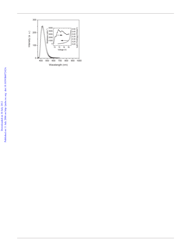
Fig. 4 Electroluminescent spectra of ED film device. Inset is the
relationship between luminance, efficiency and voltage of this device.
The ED film used in this device is prepared using deposition parameters:
scan range from 20.2 V to 0.85 V, 52 scan cycles at scan rate of 200 mV/s,
a mixture of acetonitrile and CH2Cl2 (v/v 5 3/2) as solvent, TCPC content
of 1 mg/mL and TBAPF6 as supporting electrolyte.
We are grateful for financial support from the National Science
Foundation of China (grant numbers 20474024, 20573040,
90501001, 50473001), the Ministry of Science and Technology of
China (grant number 2002CB6134003) and PCSIRT.
which require a deposition time of about 12 min. Such ED films
washed with acetonitrile and dried in a vacuum oven give a clear
surface, then the metal cathode Ba/Al is deposited on the films by
vacuum evaporation to construct a prototype electroluminescent
device (ITO/ED films/Ba/Al) (see ESI). For ED film obtained by
using TBABF4 as supporting electrolyte, the achieved maximum
luminescence and luminous efficiency are 134 cd/m2 @ 16.5 V and
0.016 cd/A @ 11 V respectively after optimizing electrochemical
parameters. For ED film obtained by using TBAPF6 as supporting
electrolyte, the device exhibited a blue electroluminescent (EL)
spectrum at lmax 427 with CIE coordinates of (0.16, 0.08), and the
achieved maximum luminance and luminous efficiency of the ED
film devices are 4224 cd/m2 @ 17 V and 0.47 cd/A @ 11.5 V,
respectively (see Fig. 4). The external quantum efficiency for this
device is 0.72%. Such device performance is significantly better
than that of a TCPC spin-coated device (ITO/PEDOT:PSS/TCPC/
Ba/Al), which has maximum luminance and luminous efficiency of
78 cd/m2 @ 7 V and 0.11 cd/A @ 4.5 V, respectively. The
improved performance in the ED film device is likely due to the
enhanced thermal stability of morphology and carriers (hole)
injection because the dimeric carbazole formed in films as a result
of electropolymerization helps hole injection and transport.
Though the obtained performance of the ED film device is the
best for a single layer OLEDs, an enhancement in brightness and
efficiency can be prefigured by utilizing multi-layer ED film
involving an emitting layer and a carrier injecting layer. Recently,
Roitman and Advincula17 showed that ED films as a hole injecting
layer can improve the performance of polymer EL devices.
Notes and references
1 P. Sigwalt, G. Wegner, J. Morin, M. Leclerc, D. Ade`s and A. Siove,
Macromol. Rapid Commun., 2005, 26, 761.
2 C. Weder, Chem. Commun., 2005, 5378.
3 H. Yu, B. Xu and T. M. Swager, J. Am. Chem. Soc., 2003, 125, 1142.
4 Y. Liu and C. Tsai, Chem. Mater., 2003, 15, 320.
5 J. L. Reddinger and J. R. Reynolds, Adv. Polym. Sci., 1999, 145, 57.
6 E. J. W. List, R. Guentner, P. Scanducci de Freitas and U. Scherf, Adv.
Mater., 2002, 14, 374.
7 P. Marrec, C. Dano, N. Gueguen-Simonet and J. Simonet, Synth. Met.,
1997, 89, 171.
¨
8 P. Damlin, T. Osterga˚rd, A. Ivaska and H. Stubb, Synth. Met., 1999,
102, 947.
¨
9 T. Osterga˚rd, C. Kvarnstro¨m, H. Stubb and A. Ivaska, Thin Solid Films,
1997, 311, 58.
10 L. M. Goldenberg, V. I. Krinichnyi and I. B. Nazarova, Synth. Met.,
1991, 44, 199.
11 W. Chang, W. Whang and P. Lin, Polymer, 1996, 37, 1513.
12 C. Xia, R. C. Advincula, A. Baba and W. Knoll, Chem. Mater., 2004,
16, 2852.
13 M. Sac¸ak, U. Akbulut, C. Cheng and D. N. Batchelder, Polymer, 1994,
35, 2495.
14 S. A. Sarac¸, E. Sezer and B. Ustamehmetoglu, Polym. Adv. Technol.,
1997, 8, 556.
15 Z. H. Wei, J. K. Xu, G. M. Nie, Y. K. Du and S. Z. Pu, J. Electroanal.
Chem., 2006, 589, 112.
16 F. Tran-Van and C. Chevrot, Electrochim. Acta, 2002, 47, 2927.
17 S. Inaoka, D. B. Roitman and R. C. Advincula, Chem. Mater., 2005, 17,
6781.
18 B. J. de Gans, P. C. Duineveld and U. S. Schubert, Adv. Mater., 2004,
16, 203.
19 Z. Shen, P. E. Burrows, V. Bulovic, S. R. Forrest and M. E. Thompson,
Science, 1997, 276, 2009.
The ED films can be addressed at a well-defined electrode
(micrometer size). It provides a new method for fabricating
micropatterned polymeric electroluminescent devices, which may
This journal is ß The Royal Society of Chemistry 2006
Chem. Commun., 2006, 3393–3395 | 3395

 Li, Mao