Chemistry Letters 2002
929
(8 Â 104 and 3 Â 105 nm3/s, respectively) independent of wire
diameter. The diameters of both types of silver nanowires are
markedly larger than the bottleneck size (around 0.26 nm) of the
Agþ ion channels in the NASICON matrix. The nanowire may
thicker at the surface of the powder with extremely fine silver
lines in the channels bundling together.
TEM observation showed that the nanowire spinning was
more vigorous when the sample was irradiated by a convergent
electron beam. This result suggests that the rate of nanowire
spinning depends mainly on the current density of the irradiating
electron beam, and not on the accelerating voltage. At a high
current density, since the nanowire spinning progresses vigor-
ously from the matrix, the nanowires are liable to bend away from
a straight line. They often bend markedly to abut on the surface of
the powder. On the other hand, the nanowire tends to elongate
slowly with less bending at a relatively low current density. Thus,
a low current density is advantageous for the formation of long
silver nanowire.
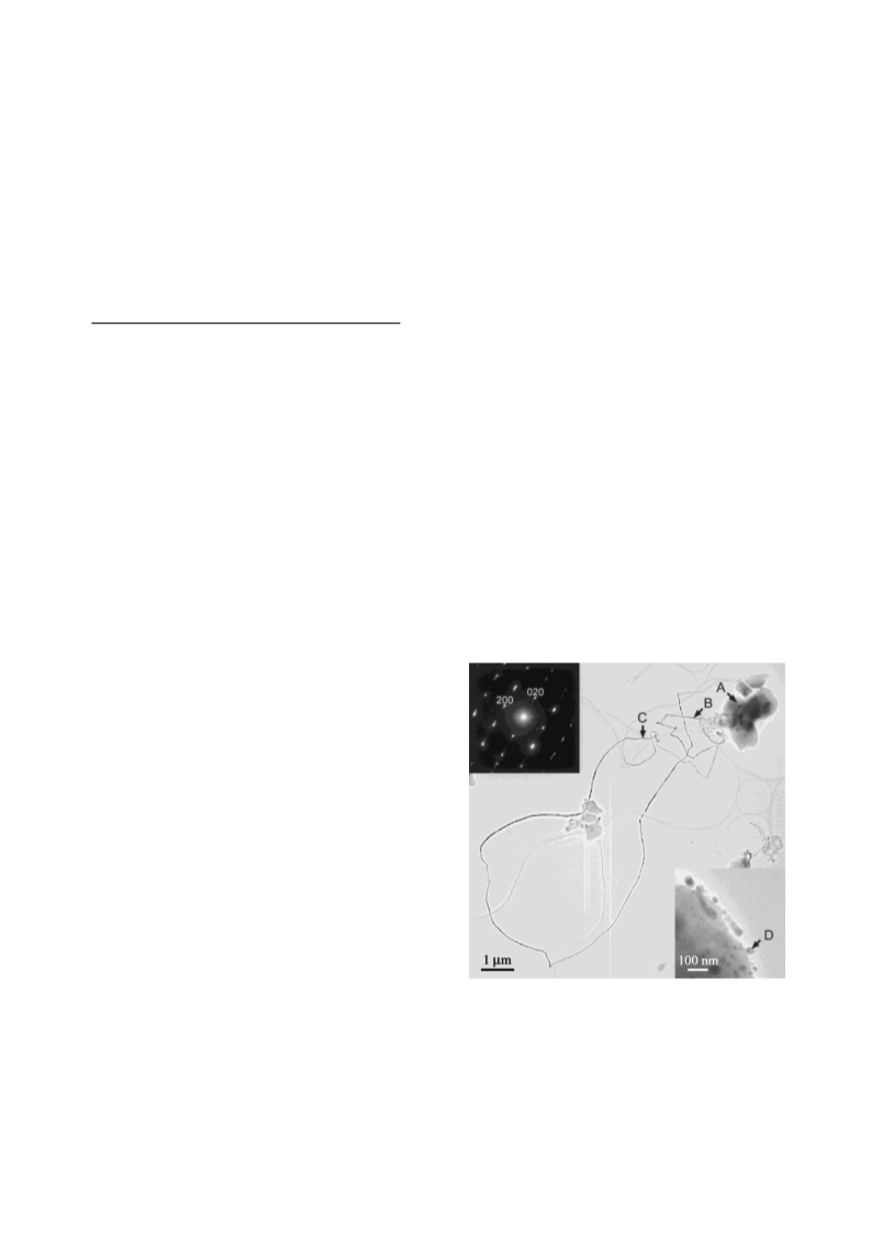
Table 1. Results of the EDS analysis on different parts (A–D) in
Figure 1
A
B
C
D
Ag
Na
Zr
Si
0.99
0.00
39.00
31.65
28.36
98.24
0.00
0.00
1.56
0.20
99.48
0.00
0.52
0.00
0.00
94.72
0.00
2.10
0.86
2.32
P
Unit: atom%
The results give the amount of atoms of all kinds excluding
oxygen in the starting material as 100 atom percent. The EDS
analysis was carried out using a convergent electron probe of
25 nm diameter.
the aspect ratio of the wire reaches more than 2000, which is, to
our knowledge, the highest among the nano-order silver wires
reported to date.
The particles after the electron beam irradiation contain little
elemental silver. The nanowire spinning proceeds steadily until
the silver element in the matrix is depleted. This suggests that the
electron beam irradiation on the matrix produces a strong force
that expels metallic silver from the matrix. The nanoparticles,
typically 5–40 nm in size, were not observed at the beginning of
irradiation, but were observed toward the end of spinning. The
nanoparticle arrowed D in Figure 1 consists almost entirely of
silver, as does the nanowire (Table 1).
Silver nanowire spinning was recognized at different
accelerating voltages of 5, 10, 20, 30, 200 and 300 kV
independent of the accelerating voltage. Two kinds of silver
nanowire, a clump of nanowires and a linear nanowire, were
typically observed as is shown in Figure 2. The very fine clump-
type nanowire of 5–15 nm in diameter appeared when it spun
vigorously outside the matrix (Figure 2a–c). The thicker linear
type nanowire, however, was revealed when it elongated slowly
from the surface (Figure 2d–f). The spinning-volume rates
estimated from in situ SEM observation were nearly equal
The silver content of the original powder is an important
factor controlling the spinning of silver nanowire. In a matrix with
smaller
silver
content
(chemical
composition
Ag0:5H1:8Na0:2Zr2Si1:5P1:5O12, silver content 10 wt%), a TEM
photograph after electron beam irradiation did not show any
nanowires, but only nanoparticles, similar to those in Figure 1,
observable on the surface of the matrix. This result suggests that
electron beam irradiation generates sufficient force to expel
elemental silver from the matrix regardless of silver content, but
there is a minimum threshold of silver content that enables the
formation of nanowire.
Silver nanowire spinning was not recognized in some kinds
of powders, Agþ-exchanged cubic antimonic acid (high Agþ
selectivity), hollandite type manganese oxide (with 2 Â 2 tunnel)
and zeolite (type A), despite their Agþ contents being markedly
high (above 10 wt%). In addition to the silver content, easy
migration of Agþ ions from inside to the surface of the powder
may be necessary for the formation of nanowire. Silver atoms
must be supplied smoothly to ion channel outlets of the powder
for the formation of silver nanowire. Materials with a NASICON
structure may be well suited for precursor to spin silver nanowire,
since they are generally good ionic conductors due to the presence
of channels through which Agþ ions can move easily.11{13
References
1
2
H. Ohnishi, Y. Kondo, and K. Takayanagi, Nature, 395, 780 (1998).
€
A. I. Yanson, G. R. Bollinger, H. E. van den Brom, N. Agraꢀt, and J. M.
van Ruitenbeek, Nature, 395, 783 (1998).
3
4
5
Y. Kondo and K. Takayanagi, Science, 289, 606 (2000).
M. H. Huang, A. Choudrey, and P. Yang, Chem. Commun., 2000, 1063.
J. Sloan, D. M. Wright, H. Woo, S. Bailey, G. Brown, A. P. E. York, K. S.
Coleman, J. L. Hutchison, and M. L. H. Green, Chem. Commun., 1999,
699.
6
7
N. R. Jana, L. Gearheart, and C. J. Murphy, Chem. Commun., 2001, 617.
S. Liu, J. Yue, T. Cai, and K. L. Anderson, J. Colloid Interface Sci., 225,
254 (2000).
8
9
C. Fan and G. Meng, J. China Uni. Sci. Tech. (in Chinese), 18(1), 139
(1988).
A. Ono, J. Mater. Sci., 19, 2691 (1984).
10 Y. Shimizu, Y. Azuma, and S. Michishita, J. Mater. Chem., 7(8), 1487
(1997).
11 H. Y. Hong, Mater. Res. Bull., 11, 173 (1976).
12 J. B. Goodenough, H. Y. Hong, and J. A. Kafalas, Mater. Res. Bull., 11,
203 (1976).
Figure 2. In situ SEM observations of a clump of nanowire
(a–c) and a thicker linear nanowire (d–f). Irradiation times of
a, b and c are 14, 40 and 392 s, respectively. Irradiation times
of d, e and f are 42, 76 and 78 s, respectively.
´
´
13 A. Martꢀnez-Juarez, C. Pecharroman, J. E. Iglesias, and J. M. Rojo, J.
ꢁ
Phys. Chem., B102, 372 (1998).

 Makita, Yoji